Polarization-induced Strain coupled Transition Metal Dichalcogenide FET (PeFET)
Introduction
Among several non-volatile memories, ferroelectric based memories show distinct advantages due to electric field-driven low-power write. However, there are other concerns in ferroelectric based non-volatile based memories such destructive read in FERAMs, gate leakage in
FEFETs with floating inter-layer metal and traps and depolarization fields in FEFETs without inter-layer metal. To overcome such issues while retaining the useful features of ferroelectric, we propose a Polarization-induced Strain coupled Transition Metal Dichalcogenide FET (PeFET).

(A) (B)
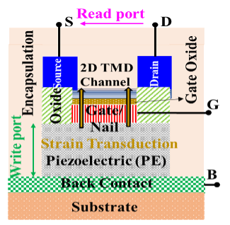
Figure 1. (A) Device structure of a PeFET showing its four terminals, namely back (B), drain (D), gate (G) and source (S). (B) Schematic of PeFET.
The device structure and schematic of PeFET is shown in Fig. 1(A,B). PeFET is 4-terminal device comprising of drain (D), gate (G), source (S) and back (B) contacts. A ferroelectric material (PZT-5H in our work) is placed between the gate and the back terminal. The channel of PeFET is composed of Transition Metal Dichalcogenide (e.g., MoS2). PeFET features (a) polarization-based non-volatile bit-storage and electric field-driven write in ferroelectric and (c) coupling of piezoelectricity with dynamic bandgap tuning of 2D Transition Metal Dichalcogenides for read.
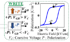
Fig. 2 Storage and write mechanism of PeFET.
The storage and write mechanism are illustrated by Fig. 2. Polarization switching, such as -P to +P or vice versa, which accounts to write operation occurs when a voltage (VGB) greater than coercive voltage (VC) is applied to the ferroelectric as shown in Fig. 2.

Fig. 3 Read mechanism of PeFET.
PeFET employs a unique read mechanism leveraging polarization-induced strain in ferroelectric/ piezoelectric subject to read voltage. The read mechanism is illustrated in Fig. 3. Strain in piezoelectric yields stress which transduces as pressure in Transition Metal Dichalcogenide channel, leading to its dynamic bandgap modulation. This tunes the drain current leading to low/high resistance states (LRS/HRS) of PeFET. For +P, we observe LRS, whereas -P shows HRS. The transfer characteristics in Fig. 4 highlight LRS (for +P) and HRS (for -P) of PeFET in terms of drain to source current (IDS). Based on our preliminary analysis, a distinguishability of 8X is observed between the two states for a read voltage of 0.4V.
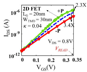
Fig. 4 Transfer characteristics of PeFET
The four terminal structure of PeFET provides avenues for designing multiple flavors of PeFET based non-volatile memories based on the requirement of applications. The PeFET device is directly deployable as a 1 transistor – 1 capacitor non-volatile memory as shown in the array below (Fig. 5). Due to its small footprint, it offers high integration density (HD). It overcomes issues of destructive read in its pure ferroelectric counterpart, FERAM. Moreover, it does not suffer from gate leakage observed in other ferroelectric based transistors (with inter-layer metal). However, the HD cell takes a hit in performance and energy consumption. To mitigate this, we are currently focusing on design of PeFET based non-volatile memories with access transistors.
Ongoing effort
Our objective is to study and benchmark area-latency-energy of various flavors PeFET based non-volatile memories against state-of-the-art SRAM. Further, we plan to implement device-optimization in PeFET that could lead to tradeoffs between distinguishability, area, latency and performance at the array level.
We have identified that the special read mechanism of PeFET enriches it as a memory inherently suitable for > binary sensing. Our ongoing effort is to leverage this feature to design PeFET based arrays for in-memory dot-product computation in > binary precision.

Fig. 5 High density PeFET based array